Powering the Next Generation of Semiconductor Innovation
The manufacturing inflection is here.
Are your process and products keeping up?
At sub-3nm logic nodes, inside increasing 3D NAND stacks, across the transition to vertical DRAM architectures, and throughout the growing silicon photonics applications, conventional reactive ion etching is hitting its limits.
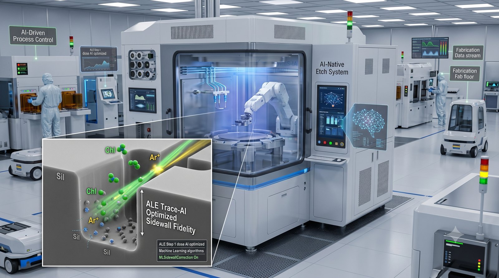
The common thread is not the device type. It is the precision requirement. At each of these inflection points, the etch step that determines yield is one that demands atomic-scale control. That is where Atomic Layer Etching (ALE) is increasing in intensity and is expected to grow by 20X over the next few years.
Four markets. One platform.
AAT's AI-native ALE platform is built to serve the etch requirements of the four segments where this shift is happening fastest. The same core technology — decoupled modification and removal steps, real-time AI process control, production-worthy cycle times — addresses a different set of manufacturing challenges in each application.
GAA & Beyond
Gate-all-around nanosheet architectures require selective removal of sacrificial layers with sub-nanometer precision. Conventional RIE cannot do this without damaging the channel. ALE is the enabling process.
Explore the segment →
3D NAND
As stack heights climb past 300 layers, precision finishing at the etch step — damage removal, selective recess, staircase cleanup — becomes yield-critical. RIE handles bulk removal; AAT handles the steps RIE cannot.
Explore the segment →
DRAM
The transition from planar to vertical channel architectures is driving a step-change in process complexity. Capacitor trench uniformity, buried bitline formation, and gate recess control all require etch precision that scales with ALE.
Explore the segment →
Silicon Photonics
Waveguide sidewall roughness is the primary performance limiter in silicon photonics fabrication. ALE smooths those surfaces to a degree that RIE cannot achieve — directly reducing optical insertion loss and improving device yield.
Explore the segment →Proven performance.
AAT's platform has been independently validated at SPIE Advanced Lithography + Patterning, demonstrating true self-limiting ALE behavior across two operating modes:
- Synergy Factor>90%
- Linearity (R²)>0.9997
- Cycle Time~2 seconds
- Synergy Factor>80%
- Linearity (R²)>0.9947
- Cycle Time~2 seconds
Both modes operate in the same chamber, switched algorithmically based on the process requirement. No tool changeover. No separate qualification.
Source: SPIE Advanced Lithography + Patterning 2026, Paper 13984-24