Silicon Photonics
Experience the surface precision that brings high-performance AI optical interconnects to life
- Co-packaged optics
- WDM transceivers
- Photonic ICs
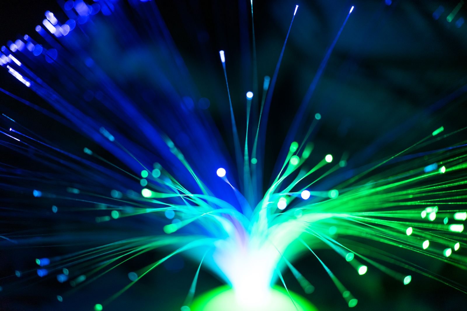
In photonics, surface quality is the product.
Sidewall roughness sets the propagation-loss floor.

AI is pushing data centers beyond the bandwidth limits of copper – and silicon photonics is the answer. The surface quality that makes photonic devices perform starts at the etch step. A single atomic defect on a waveguide sidewall scatters light. At scale, that scattering translates directly into insertion loss and insertion loss determines whether a photonic device meets its performance spec or not. Atomic-level etch control is not a nice-to-have here. It is the enabling step.
As AI infrastructure leans harder on optics, the etch surface stops being a process detail and becomes a competitive one. The teams that treat surface finishing as a first-class step — not an afterthought — set the performance ceiling everyone else designs against.
Where AAT Fits
Silicon photonics is moving from research fabs into volume production, driven by the explosion in AI data center demand for optical interconnects. Co-packaged optics, high-density WDM transceivers, and photonic integrated circuits all require waveguides with sidewall roughness at the sub-nanometer scale.
Conventional RIE leaves nanometer-scale line edge roughness on waveguide sidewalls. That roughness causes light scattering – a phenomenon that compounds across the length of the waveguide and limits how tightly components can be packed on a photonic chip. It is the primary yield and performance limiter in silicon photonics fabrication today.
AAT's isotropic ALE mode is used as a post-RIE finishing step on waveguide sidewalls, grating coupler structures, and other photonic features where surface quality directly determines optical performance. ALE smooths surfaces to a degree that RIE cannot achieve, directly reducing propagation loss and improving device yield.
Demonstrated Performance
- Synergy Factor>80%
- Linearity (R²)>0.9947
- Cycle Time~2 seconds
- Modification saturation~2.0 Å at 1 second
- Removal saturation~2.1 Å at 1 second
Self-limiting saturation confirmed at ~1 second for both steps — providing the repeatability that photonic device yield requires.
Source: SPIE Advanced Lithography + Patterning 2026, Paper 13984-24
The AAT Advantage
Sub-nanometer surface control.
AAT's precision mode operates at 2.34 Å per cycle with confirmed self-limiting behavior. At that scale, the tool is conditioning the surface, cycle by cycle, to a quality level that no continuous etch process can match.
Fast enough for production.
~2 second cycle time means atomic-level surface finishing does not need to be a bottleneck in your photonics process flow.
Active customer engagement.
AAT is currently in active process development engagement with a leading photonics foundry.