// Careers

Make your work matter at the atomic scale.

We are solving one of the hardest problems in semiconductor manufacturing, and we are doing it with a small, highly experienced team that moves at startup speed. If you want your work to matter at the atomic scale, this is the place.

// Life at AAT

Life at AAT

At AAT, there are no large org hierarchies slowing things down. We are an AI-native organization where agents are adopted as work mates — every engineer and scientist is amplified by AI that handles the routine so you can focus on the hard problems. You will work directly with the founders, contribute across disciplines, and see the impact of your work in days not quarters. We are a team of engineers and scientists who take the science seriously and the bureaucracy lightly.

We are based in Singapore's One-North innovation district, one of Asia's most dynamic deep-tech ecosystems, with access to world-class research institutions; and our Yishun site is in a thriving semiconductor technology park, surrounded by world-class companies in the semiconductor ecosystem.

// Why AAT?

Why AAT?

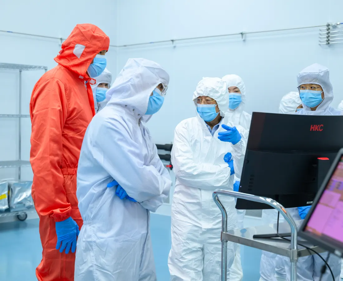
Atomic-scale etch platform in development at AAT01

Work on something genuinely new

AAT is building the world's first AI-native atomic layer etching platform. A clean-sheet design, built for a process that the semiconductor industry now depends on — and we are the only company that started here.

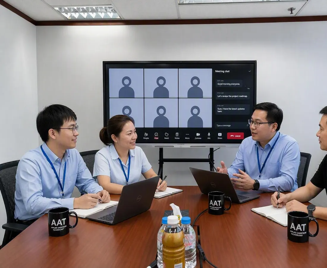
AAT's engineering and science team at work02

Work with people who have done it before

Our team brings 100+ combined years of experience in semiconductor industry from Applied Materials, Lam Research, Intel, GlobalFoundries. The founders have shipped several industries first products into high-volume manufacturing. You will learn fast here.

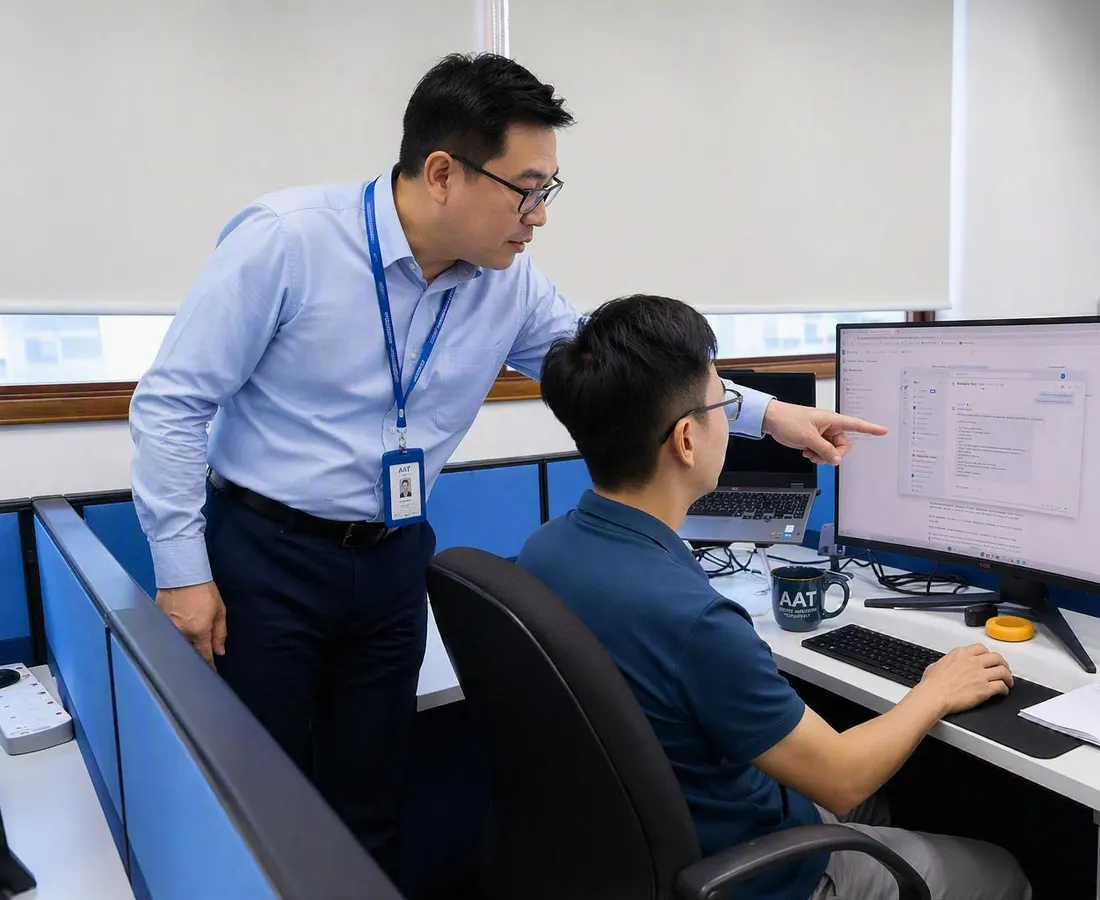
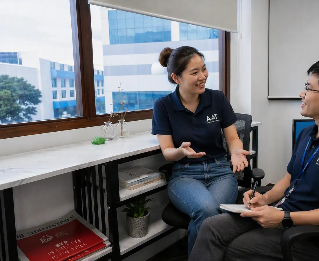
Collaborative, hands-on work environment at AAT03

Work in an environment built for growth

We offer a flexible, collaborative, and supportive work environment where people are trusted to do their best work. We invest in internal training and mentorship, and we give people the opportunity to work across functions — hardware, software, process, and business — in ways that are rare at larger companies.

Precision hardware and AI-native process control at AAT04

Work at the intersection of deep tech and AI

AAT's platform sits at the crossroads of precision hardware engineering and AI-native process control. Whether you are a process engineer, a hardware designer, or a software engineer, you will be working on problems that connect directly to the chips powering the next generation of AI infrastructure.

// Open Roles

Open Roles

We're hiring across engineering and automation. Expand a role to read the full description, then apply directly by email.

As a Senior RF Engineer at AAT, you will operate at the critical intersection of high-frequency power electronics and advanced plasma physics. You will serve as the technical authority for AAT’s RF delivery architecture, driving clean-sheet design, dynamic impedance matching, and plasma source characterization to enable sub-angstrom profile precision in next-generation Atomic Layer Etching (ALE) chambers.

What You'll Do

  • Support RF & Plasma tool development/qualification and implementation in Plasma Etch chambers for R&D and Production applications
  • Conduct experiments and characterizations of RF & Plasma systems and components at bench and tool levels using various instruments including Network Analyzers, Spectrum Analyzer, Plasma Probes, analog and digital data acquisition controllers.
  • Develop new methods to distribute RF through antennas and networks to ignite stable plasmas using different frequency and Generators.
  • Develop new RF & Plasma arc detection and diagnostic methods to be used in R&D and Production applications.
  • Work with Process Engineers and Field/Customer support teams to provide RF & Plasma support to quickly troubleshoot and resolve field/customer issues.

Job Description

  • Masters or PhD in science or engineering areas with emphasis on high frequency electronics or plasma physics.
  • Experience with a wide range of plasmas (DC~MW, various pressure and gas conditions).
  • Knowledge of unique challenges in large area plasma production and the techniques used in the industry.
  • Knowledge in plasma diagnostics (Langmuir probes, optical diagnostic, microwave diagnostic etc.).
  • Knowledge in Etch or CVD technology, applications, and film metrology.
  • Experience in mechanical design (manufacturability, mechatronics, material properties, vacuum systems, gas flow etc.)
  • Experience with system design and module integration on system level (PLCs, IoT, Edge, safety)
  • Solid background in RF power delivery, impedance matching, RF sensors, transmission line theory, electronic circuits, amplifiers, sensors etc.
Apply now Open your email app — attach your resume before sending.

// Get in touch

Don't see the right role listed?

We are always interested in hearing from exceptional people with semiconductor equipment, process, or AI backgrounds. Reach out to us and tell us what you would bring to the team.

Email careers @ aatech.sg →
// Get in touch

Deep expertise. Startup speed. Real results

Talk to our team about process development, equipment demonstration, or partnership opportunities.